PCI Express I/O System
Table of Contents
I/O Hardware Overview #
The basic I/O hardware elements, such as ports, buses, and device controllers, accomodate a wide variety of I/O devices.
To encapsulate the details and oddities of different devices, the kernel of an operating system is structured to use device-driver modules.
A device communicates with a computer system by sending signals over a cable or through the air.
- The device communicates with the machine via a connection point, or port.
- If devices share a common set of wires, the connection is called a bus. (e.g. PCI bus)
- A controller is a collection of electronics that can operate a port, a bus, or a device.
How can the processor give commands and data to a controller to accomplish an I/O transfer? The short answer is that the controlelr has one or more registers for data and control signals.
Two ways in which this communiation can occur:
- Use of special I/O instructions that specify the transfer of a byte or word to an I/O port address. The I/O instruction triggers bus lines to select the proper device and to move bits into or out of a device register.
- Using memory-mapped I/O. The device-control registers are mapped into the address space of the processor. The CPU executes I/O requests using the standard data-transfer instructions to read and write the device-control registers at their mapped locations in physical memory.
NVIDIA GPU on PCI Express #
The current form of the GPU is a PCI express device. The NVIDIA GPU exposes the following base address registers (BARs) to the system through PCI in addition to the PCI configuration space and VGA-compatible I/O ports.
- BAR0
- Memory-mapped I/O (MMIO) registers
- BAR1
- Device memory windows.
- BAR2/3
- Complementary space of BAR1.
- BAR5
- I/O port.
- BAR6
- PCI ROM.
- This information is from ‘Implementing open-source CUDA runtime’. I don’t understand why they used BAR numbers 0~3, 5, and 6. Typically the BAR numbers are from 0 to 5 (total 6 BARs).
- I think PCI ROM address is not saved in the base address registers. Will be explained later.
BARs are standard registers and specified in PCI express configuration space header (type 0) as follows. Each BAR is 32-bit wide registers (BAR0: 10h~14h, BAR1: 14h~18h, etc).

The most significant area is the BAR0 presenting MMIO registers. This is the main control space of the GPU, through which all hardware engines are controlled.
Here is the GPU information provided by lspci command that I am using.
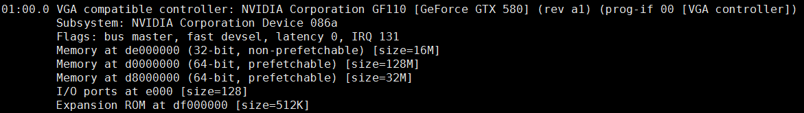
BAR0: 0xde000000 (MMIO registers)
BAR1 and BAR2: 0xd0000000 (device memory windows? 64-bit memory-map uses two adjacent BARs)
BAR3 and BAR4: 0xd8000000 (device memory windows? 64-bit memory map)
BAR5: 0xe000 (I/O ports)
PCI Expansion ROM address 0xdf000000 is saved in 30h~34h (Expansion ROM Base Address) in configuration space header, not BAR 6, as explained in ‘Implementing open-source CUDA runtime’.
References #
- Silberschatz A, Galbin P.B, Gagne G, Operating System Concepts, Wiley, 2012, ISBN:9781118063330
- PCI SIG, PCI Express Base Specification Revision 3.0, 2010
- Root Complex, Wikipedia [Online] https://en.wikipedia.org/wiki/Root_complex
- PCI configuration space, Wikipedia [Online] https://en.wikipedia.org/wiki/PCI_configuration_space
- Kato S, Implementing open-source CUDA runtime, In Proceedings of the 54-th Programming Symposium, 2013